
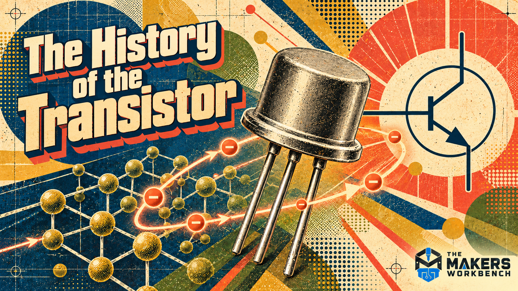
The transistor is the switch and amplifier beneath modern electronics. A small discrete transistor can turn on a relay or strengthen a sensor signal. Billions of microscopic transistors inside a processor can execute software, store data, and draw an entire digital world on a screen.
That range grew from a difficult materials problem. Engineers understood the goal before they could build the device. The first working transistor used two gold contacts pressed against germanium in December 1947. The more durable junction transistor followed, silicon replaced germanium in demanding applications, and the planar process turned individual devices into manufacturable integrated circuits.
The three-legged transistor on a workbench hides most of the work that made it possible. This article follows that work from the early patents through the first working devices, the move to silicon, and the planar process that made integrated circuits manufacturable.
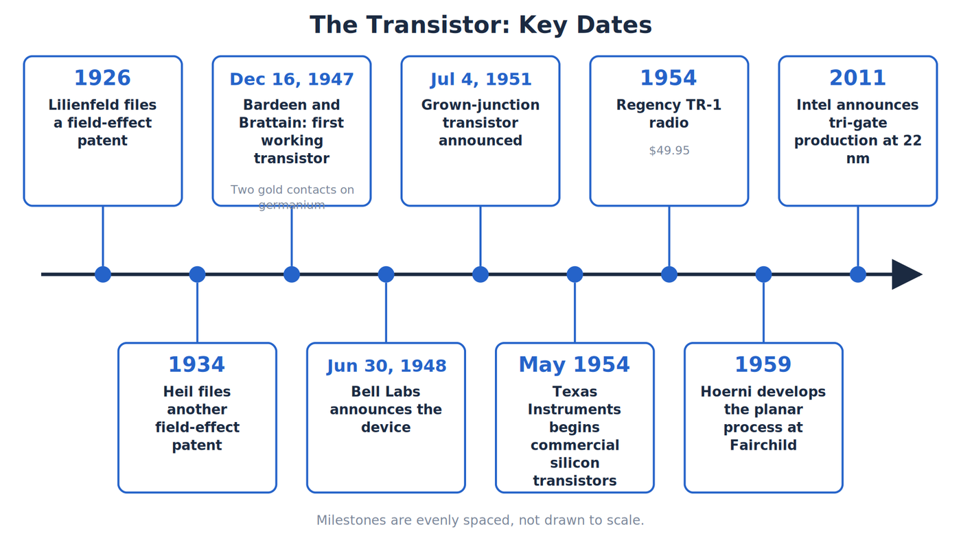
Key dates in the story of the transistor. Credit: The Makers Workbench.
The device that existed first on paper
Julius Edgar Lilienfeld filed a field-effect transistor patent in 1926. Oskar Heil filed another field-effect patent in 1934. These inventions described controlling current in a semiconductor with an electric field, an idea close to the field-effect transistors that dominate modern chips.
The patents did not produce a documented working commercial device. The semiconductor surface trapped electrical charge and disrupted the field that was supposed to control current inside the material. Bell Labs researchers encountered that obstacle directly in the 1940s.
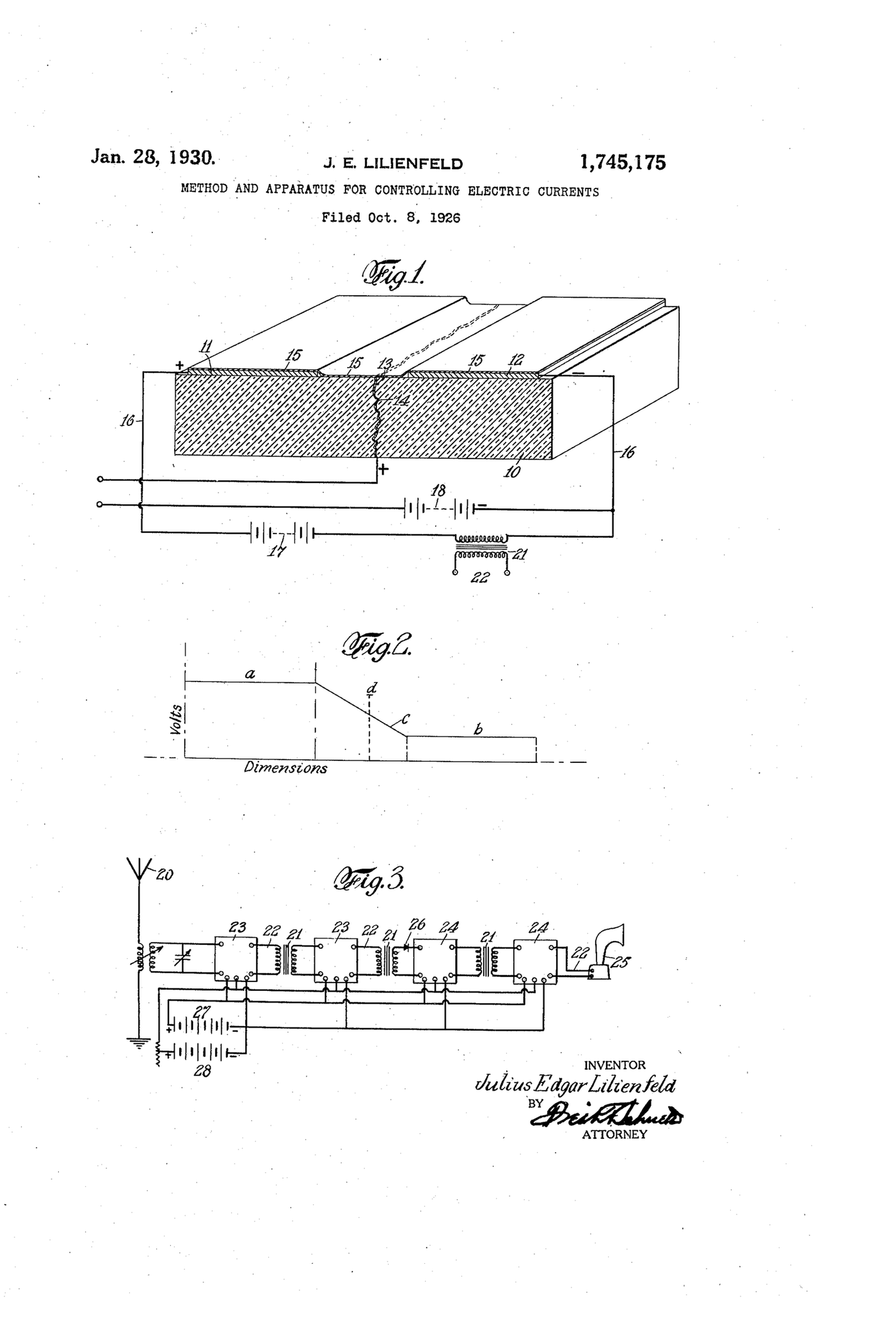
Lilienfeld's patent drawings (filed in 1926, granted in 1930) for controlling current with a field. Credit: US Patent 1,745,175, page 1.
This distinction keeps the history honest. A patent can establish an early concept without proving that the inventor built a practical transistor. The theory came first, while materials purity, surfaces, and manufacturing had to catch up.
Two gold points on germanium
Bell Labs formed a solid-state research group led by William Shockley. Physicist John Bardeen studied surface states, the trapped charges that helped explain why the field-effect approach was failing. Experimental physicist Walter Brattain built and tested devices.
Their work took place inside a much larger effort to replace the vacuum tube in telephone systems. Tubes could amplify signals, but they consumed power, produced heat, and eventually failed. A nationwide network containing vast numbers of repeaters and switches turned those weaknesses into maintenance costs. Bell Labs wanted a smaller solid-state amplifier that could last longer and use less energy.
On December 16, 1947, Bardeen and Brattain achieved power gain with two closely spaced gold contacts pressed onto a germanium crystal. One contact injected charge carriers and the other collected them. A third connection to the germanium acted as the base.
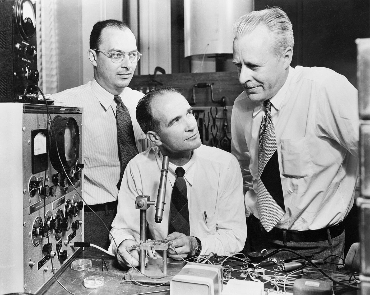
A Bell Labs publicity photograph of Bardeen, Brattain and Shockley. Credit: AT&T / Bell Labs publicity photograph, photographer stamped as Jack St., New York. Wikimedia Commons, File:Bardeen_Shockley_Brattain_1948.JPG.
They demonstrated the point-contact transistor to Bell Labs officials on December 23. It could amplify an audio-frequency signal. Bell Telephone Laboratories publicly announced the device on June 30, 1948.
Shockley led the group, but he did not invent that point-contact device. Bardeen and Brattain did. Shockley later acknowledged both his excitement and his frustration at not being one of its inventors. That frustration pushed him toward a different structure. The name "transistor," a blend of "transfer" and "resistor," was proposed by John R. Pierce and chosen by an internal vote at Bell Labs in 1948. Shockley, Bardeen, and Brattain shared the 1956 Nobel Prize in Physics for the invention.
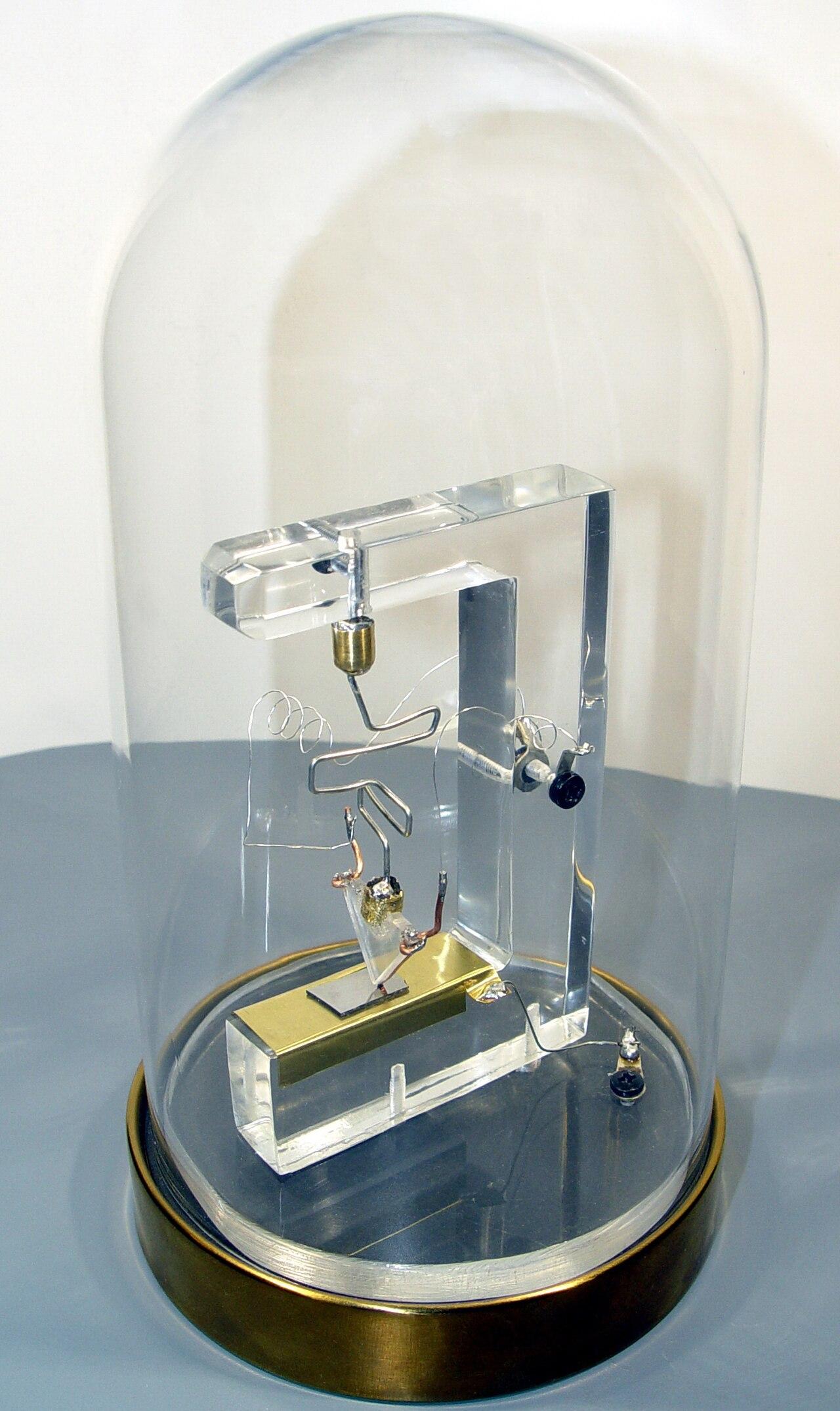
A replica of the first working transistor: a plastic wedge, metal points and a germanium slab. Credit: “A replica of the first working transistor,” Mister rf, CC BY-SA 4.0, https://commons.wikimedia.org/wiki/File:A_replica_of_the_first_working_….

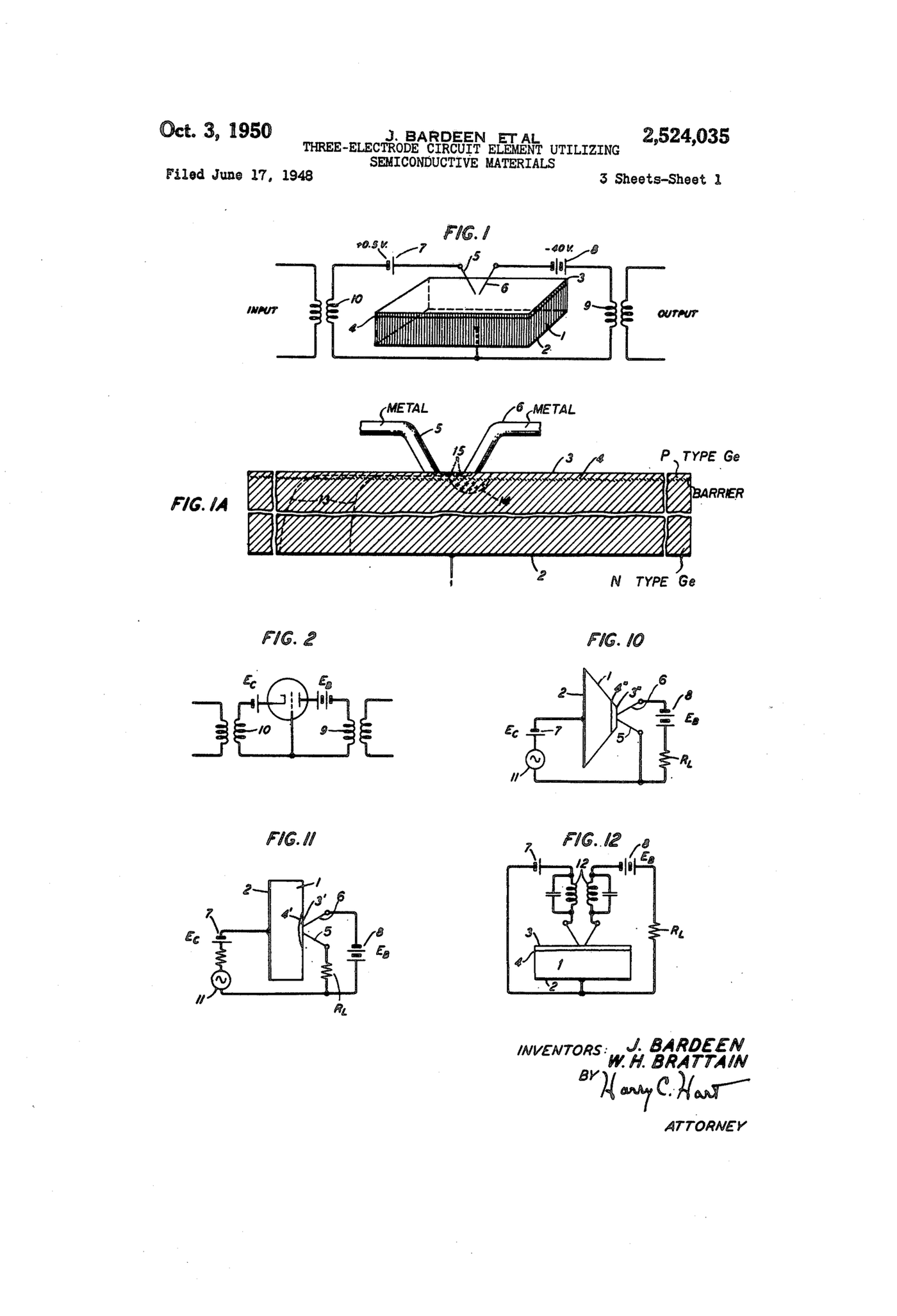
Sheet 1 of the Bardeen and Brattain patent, with the point-contact structure in Fig. 1A. Credit: US Patent 2,524,035, page 1.
The junction transistor
In January 1948, Shockley conceived the junction transistor. Instead of relying on two metal points touching a semiconductor surface, it used adjoining semiconductor regions. The important boundaries between those regions are p-n junctions, places where p-type and n-type material meet.
In a bipolar junction transistor, a small current through the base controls a larger current between the collector and emitter. “Bipolar” means both electrons and holes participate in conduction. An NPN transistor and a PNP transistor use opposite arrangements of doped regions and opposite polarities, but the control idea is related.
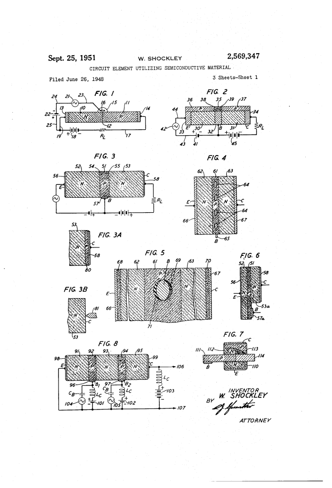
Sheet 1 of Shockley's junction patent. Credit: US Patent 2,569,347, page 1.
The first concept still had to become manufacturable. Gordon Teal and Morgan Sparks grew junction structures in germanium, and Bell Labs announced the grown-junction transistor on July 4, 1951. It was more rugged and reproducible than the delicate point-contact arrangement.
The point-contact and junction devices also controlled current in different ways. In the point-contact device, the two closely spaced contacts altered charge flow near the germanium surface. The geometry was difficult to reproduce and sensitive to the exact pressure and spacing of the contacts. A junction transistor built the active regions into the semiconductor itself, which gave manufacturing a clearer path toward repeatable electrical behavior.
An independent European line developed at nearly the same time. Herbert Mataré and Heinrich Welker built a point-contact amplifier in France in June 1948. Devices from their work entered French telephone service by 1949, and their company Intermetall publicly demonstrated a transistor radio in Düsseldorf in 1953. The Bell Labs invention remains central, but the European work prevents the early commercial history from being reduced to one laboratory and one country.
Germanium was the practical starting material, but it has relatively high leakage current and its behavior changes strongly with temperature. Silicon offered better high-temperature performance and lower leakage once manufacturers learned to purify and process it. Morris Tanenbaum built the first working silicon transistor at Bell Labs in January 1954, a few months before Gordon Teal's work at Texas Instruments. Texas Instruments was first to put commercial silicon transistors into production, in May 1954. In 1955, Tanenbaum and Calvin Fuller introduced gaseous diffusion for doping silicon, a technique that gave manufacturers precise control of the junctions.
Silicon was harder to refine and work with at first, so germanium did not disappear overnight. Early hearing aids and radios used germanium because it was available and could operate at low voltages. Silicon became increasingly valuable as circuits faced heat, higher power, and tighter reliability requirements. The material transition followed manufacturing capability and application needs rather than a single clean replacement date.
Bell opens the door
Bell Labs could have kept transistor knowledge close, but it licensed the technology broadly. In 1952, companies paid $25,000 to attend a transistor symposium and receive a license package. More than 40 companies participated.
The April 1952 program lasted nine days. Bell Labs engineers explained device theory and manufacturing techniques, while the license opened access to the patent portfolio. The fee was an advance against royalties rather than the purchase of one secret recipe. Participating companies left with enough knowledge to begin their own difficult process development.
That transfer mattered because the transistor was not a single drawing that any factory could copy. Manufacturers needed knowledge about crystal growth, purification, contacts, packaging, testing, and circuit use. The symposium and licensing program helped move that practical knowledge into a growing semiconductor industry.
Licensees still had to build their own production expertise. Crystal furnaces, furnaces for diffusion, chemical processing, clean assembly, and electrical test all affected yield. Yield is the share of manufactured devices that meet the required specifications. A transistor that worked once in a laboratory had been invented. An industry required a production line that turned out thousands of consistent devices at an affordable cost.
Western Electric's Allentown plant started the first commercial transistor production line in 1951, and the first commercial telecommunications use came in 1952, in tone generators for a crossbar switching system.
Texas Instruments and the company that became Sony were among the businesses that built on the opportunity. Competition drove new structures, better yields, and falling prices.
Sony's founders approached the license from a very different starting point. Masaru Ibuka learned of the Western Electric offer during a 1952 trip to the United States, and Akio Morita later traveled to sign the agreement. Their company did not yet have a mature transistor factory. It had to learn semiconductor production while also designing a product that consumers would want.
At Texas Instruments, Gordon Teal brought expertise in grown crystals from Bell Labs. A working TI silicon transistor appeared in April 1954, and Teal announced the technology in Dayton on May 10. Later that month, company president Patrick Haggerty demanded a transistor-radio prototype on an extremely short schedule. TI then partnered with Industrial Development Engineering Associates, or IDEA, which sold the finished radio under the Regency name.
Hearing aids and pocket radios
Hearing aids became one of the earliest successful consumer uses. They needed small, low-power amplifiers and could justify the high price of early transistors. By the early 1950s, hybrid hearing aids combined transistors with miniature vacuum tubes, and fully transistorized models followed.
In 1953, Raytheon's CK722 became an affordable transistor aimed at hobbyists, which put the part into the hands of experimenters and not only manufacturers.
The pocket radio made the technology visible. Regency introduced the TR-1 in the United States in 1954 for $49.95. Its four germanium transistors forced clever compromises because transistors were still expensive. The radio was important, but calling it the world's first transistor radio needs a qualification. Intermetall publicly demonstrated a transistor radio in Düsseldorf in 1953.
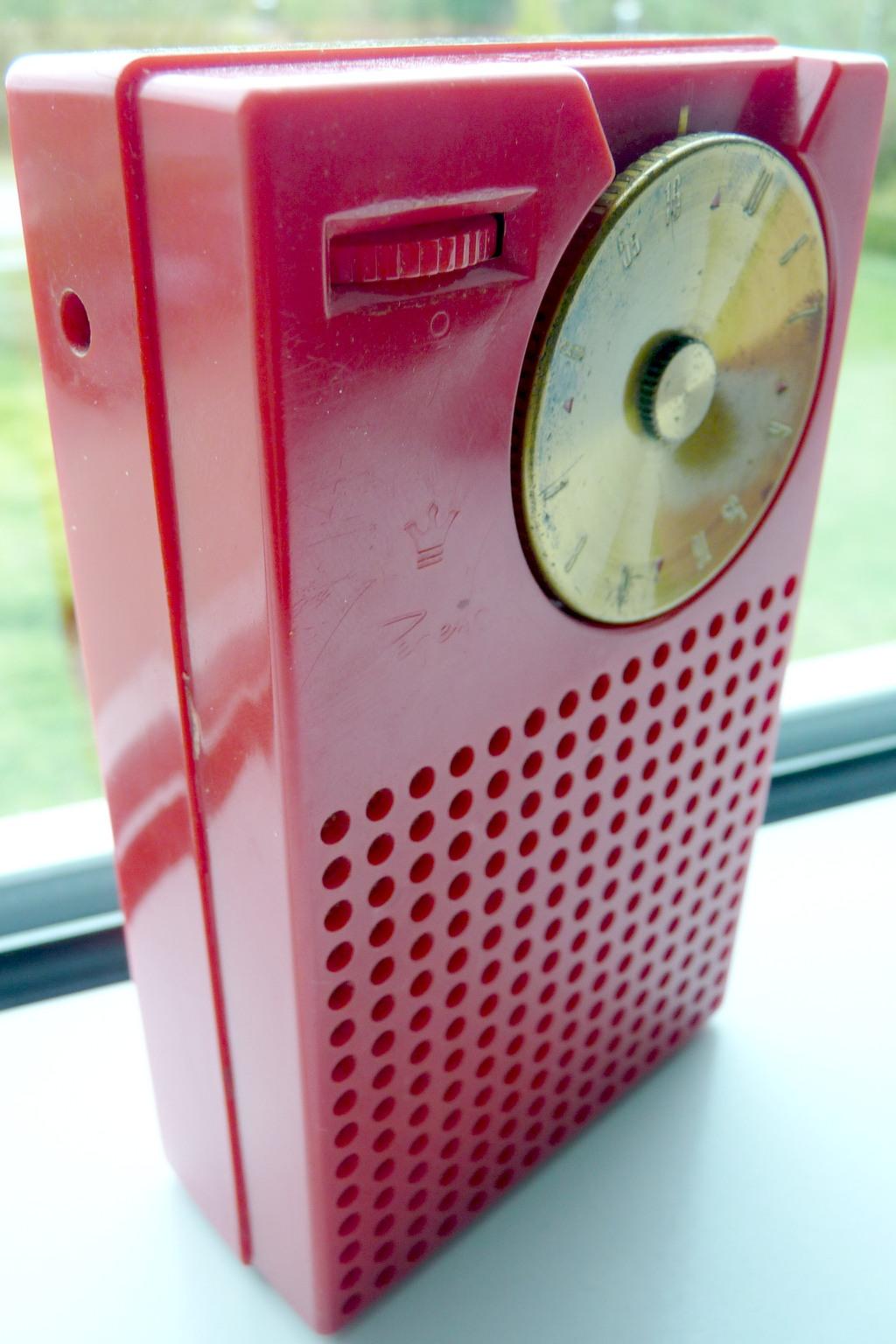
A red Regency TR-1 pocket radio. Credit: Cmglee, CC BY-SA 3.0, https://commons.wikimedia.org/wiki/File:Regency_TR-1.jpg.

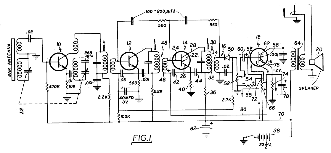
The Regency TR-1 schematic as shown in its patent. Credit: Fig. 1, US Patent 2,892,931, R. C. Koch / I.D.E.A. (USPTO, via Wikimedia Commons).
Sony's path contains another common mix-up. The TR-52 was a prototype whose decorative grille warped, so it was withdrawn. Sony sold the TR-55 in Japan in 1955. Sources differ between August and September for its introduction, and the company history supports September. The safe point is that Japanese manufacturers quickly turned the transistor radio into an international consumer product. Sony's TR-63, released in 1957, became the first mass-produced transistor radio.
Computers and telephone systems followed a similar path on a larger scale. Early transistorized machines proved that solid-state switching could replace vacuum tubes in logic while reducing heat and maintenance. The University of Manchester demonstrated a transistor computer in 1953, and Bell Labs' TRADIC followed as an important military development. By 1960, new computer designs were increasingly transistorized. The IBM 7070 and 7090 and the CDC 1604, sold between 1958 and 1960, were among the first transistorized computers offered as products.
The Manchester prototype used 92 point-contact transistors and 550 diodes. TRADIC used about 700 point-contact transistors and more than 10,000 diodes while consuming less than 100 watts. The TX-0 at MIT Lincoln Laboratory used fast germanium switching transistors and ran at 5 megahertz. These machines were small only in comparison with tube computers, but they proved that transistors could build complete digital systems.
Telephone switching provided another natural destination. Point-contact devices entered specialized switching equipment, and the Bell System placed the No. 1 Electronic Switching System into commercial service in 1965. The network problem that had motivated Bell's research was finally being rebuilt around solid-state electronics.
These systems used thousands of discrete devices and connections. They were more reliable than tube machines, but wiring and packaging still set a practical limit. That pressure made the integrated circuit a natural next step. The transistor solved the active-device problem, then exposed the interconnection problem.
From grown junctions to flat silicon
Early junction transistors were manufactured as individual structures. For electronics to become smaller and cheaper, factories needed a process that could form many reliable devices on a wafer and connect them with repeatable patterns.
Work at Bell Labs had already shown what the planar idea needed. Between 1955 and 1957, Carl Frosch and Lincoln Derick found that a layer of silicon dioxide grown on silicon protected the surface and could block diffusion where it was not wanted, and they built the first planar transistors. The oxide layer was the key that Fairchild's process later turned into a manufacturing method.
The mesa process etched raised transistor structures but left vulnerable junction edges exposed. At Fairchild Semiconductor, Jean Hoerni developed the planar process in 1959. A protective silicon-dioxide layer remained on the surface while openings in that oxide guided diffusion and later electrical connections.
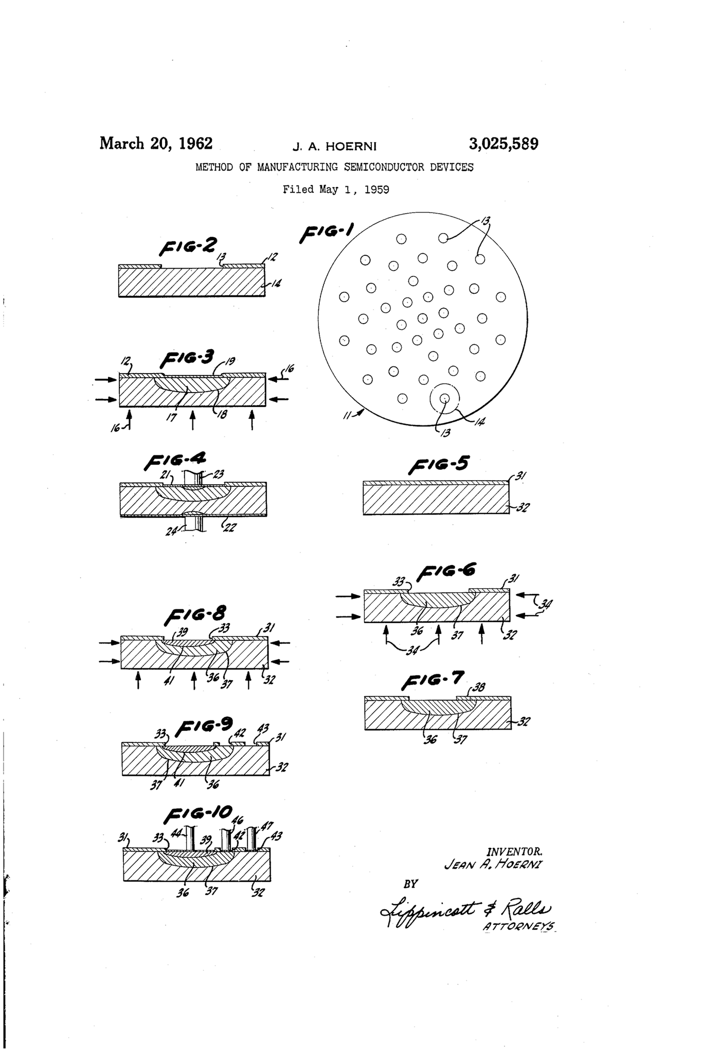
Sheet 1 of Jean Hoerni's planar-process patent. Credit: US Patent 3,025,589, page 1.
The planar process supported Robert Noyce's practical monolithic integrated-circuit concept. Monolithic means the components and their interconnections are formed together on one piece of semiconductor. Jack Kilby at Texas Instruments had already demonstrated a working integrated circuit in 1958 using external flying wires. Noyce's metal interconnections over the oxide supplied a more manufacturable structure. The companies eventually cross-licensed their work.
Fairchild itself grew from another turning point. Eight members of Shockley Semiconductor Laboratory left in September 1957 and founded Fairchild Semiconductor. Their company became a center of planar silicon development and helped seed the cluster of semiconductor firms later called Silicon Valley. The personal conflict attracts attention, but the technical result matters more here: a team with device experience built the manufacturing process that let transistors multiply on one wafer.
Fairchild's early business shows why military and computer customers mattered. In 1958, IBM's Federal Systems Division ordered 100 high-voltage silicon transistors at $150 each for a B-70 computer memory. Military programs could justify prices that consumer radios could not, giving a new manufacturer room to improve its process before costs fell.
The company's 2N697 mesa transistor reached the market in 1958, but the exposed edges of a mesa junction could be contaminated or shorted. Hoerni's planar process kept a protective oxide over the junction and brought contacts through controlled openings from the top. A working planar transistor followed in March 1959, and Fairchild introduced the 2N1613 planar device in April 1960.
At Bell Labs, Mohamed Atalla and Dawon Kahng demonstrated the metal-oxide-semiconductor field-effect transistor, or MOSFET. Computer History Museum material describes the device as achieved in 1959 and demonstrated in 1960. The MOSFET returned to the field-control principle that surface problems had blocked in 1945, now using a carefully controlled oxide interface.
The MOSFET's insulated gate draws very little steady control current. That characteristic made it especially suitable for dense digital logic. Complementary MOS, shortened to CMOS, pairs devices so that a well-designed logic gate consumes little static power while it holds a state. Improvements in geometry and manufacturing then allowed enormous numbers of switches to share a chip without requiring enormous power.
This was the point where the history of the transistor and the history of computing became inseparable. Memory, processors, image sensors, and communication chips all depended on the ability to form, connect, and test vast numbers of small devices together.
The first integrated circuits were far from cheap. Texas Instruments sold its Type 502 binary flip-flop in 1960 for $450. That price bought only a small logic function, but it demonstrated that a complete circuit could be manufactured as a product. Once planar processing, photolithography, and yields improved, adding more transistors to the same die became more economical than wiring equivalent discrete parts by hand.
MOS technology also needed time to mature. The first Bell device was slow, and the telephone system did not urgently require it. Commercial MOS parts appeared in the mid-1960s, with p-channel devices initially easier to manufacture and n-channel devices offering higher speed. Complementary circuits later paired both polarities to reduce static power, creating the CMOS foundation beneath modern digital systems. Chih-Tang Sah and Frank Wanlass at Fairchild published the CMOS circuit concept in 1963.
Memory followed the same path. In 1967, Robert Dennard at IBM patented a dynamic RAM cell built from a single transistor and a capacitor, a design still the basis of the main memory in computers. That year Dawon Kahng and Simon Sze at Bell Labs also described the floating-gate MOSFET, the structure behind flash memory.
A family rather than one transistor
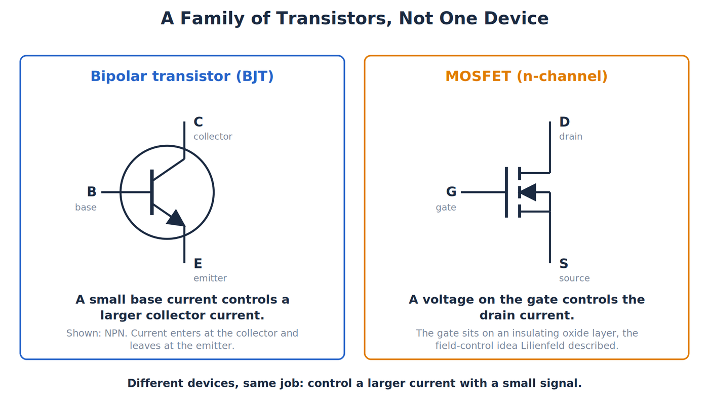
The bipolar transistor and the MOSFET, the two best-known members of the family. Credit: The Makers Workbench.
“Transistor” now names a large family. Bipolar junction transistors remain useful for amplification and switching. MOSFETs dominate digital integrated circuits and many power applications. Insulated-gate bipolar transistors, called IGBTs, combine gate control resembling a MOSFET with conductivity suited to high-power switching. Specialized radio-frequency, sensing, photonic, and high-voltage devices extend the family further.
Power devices show why one structure cannot serve every job. A processor transistor switches tiny currents at extreme density. A motor-control transistor must withstand voltage, carry substantial current, and remove heat. An IGBT may switch an inverter or industrial drive where efficiency at high voltage matters more than microscopic size. These devices share ancestry, but their physical dimensions and design priorities differ radically.
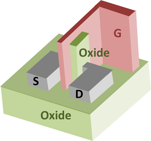
A schematic of a FinFET: one fin with oxide, gate, source and drain. Credit: Brews ohare, CC BY-SA 3.0, https://commons.wikimedia.org/wiki/File:FINFET_MOSFET.png.

Even discrete bipolar transistors divided into distinct roles. Small-signal parts emphasized gain, low noise, and modest current. Power transistors used larger junction areas and packages that could conduct heat into a heatsink. Radio-frequency devices minimized internal capacitance and carrier transit time. The word “transistor” became a category as broad as “engine,” with structures optimized for jobs that sometimes shared little beyond controlled current flow.
The physical shape has changed too. In 2011, Intel announced production technology using a three-sided “tri-gate” transistor at a 22-nanometer process node. A nanometer is one billionth of a meter. The gate wrapped around a raised fin on three sides to improve control as transistors became extremely small. Related industry terminology includes FinFET, but Intel's announcement itself used “tri-gate,” so the two labels should not be carelessly substituted in a historical quotation.
The transistor in a maker's drawer
The history can feel remote until you pick up a 2N3904. This common NPN transistor still handles small switching and amplification jobs on a breadboard. Research completed in October 2026 found individual listings around 15 to 55 cents, depending on seller and quantity.
That part and a processor transistor share the same broad purpose, controlling current, but they are very different manufactured objects. The 2N3904 is packaged as one accessible device with leads. A modern processor contains vast numbers of tightly integrated field-effect transistors that cannot be treated as individual bench parts.
The transistor's history is therefore a sequence of solved constraints. Lilienfeld and Heil described field control before surfaces allowed it. Bardeen and Brattain made the first working amplifier with gold points and germanium. Shockley developed the junction principle. Teal and Sparks made it manufacturable. Silicon improved temperature performance. Hoerni's planar process and Noyce's interconnection scheme made large-scale integration practical. The MOSFET then supplied the device structure that could be repeated on an extraordinary scale.
By one estimate from 2018, about 13 sextillion MOS transistors had been manufactured by then, more than any other human-made object.
Every modern electronics project depends on that chain, whether it uses one transistor to drive a motor or billions to run a computer.